
Under "Orcad Family Release 9.2 Lite Edition" select "Capture CIS Lite Edition". In Orcad Capture click on "File", then "New"", and "Project...". You should see a screen similar to the following.
If you want to run PSpice later, make sure the "Analog or Mixed A/D" radio button is selected. Choose a directory and a filename and click "OK". Select "Create a blank project" in the following window.

Now you should be ready to enter the schematic of a circuit.
The figure below shows the blank schematic page after creating a new project in Orcad Capture.

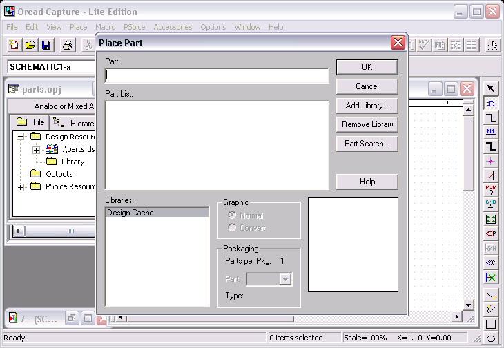
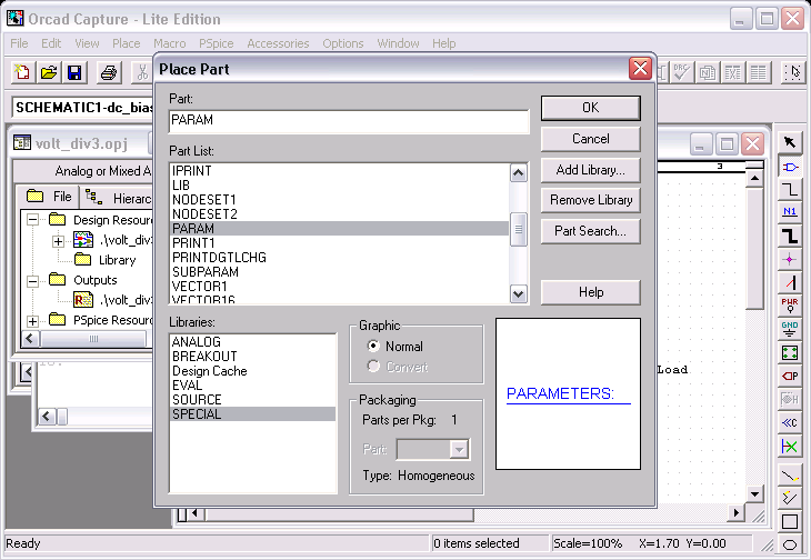
To draw a circuit, parts are placed on the schematic and then connected by wires. Parts are organized in libraries which are added to your project as you go along. Click on "Place" and select "Part..." to obtain a window similar to the following.
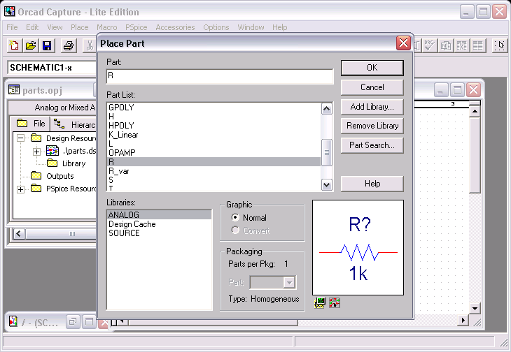
Before a part can be selected, its library (located at Orcad92Lite/Capture/Library/PSpice) must be added to the project. For the circuits 1 and 2 classes the most important libraries are "analog.olb", "eval.olb", and "source.olb". The following figure shows the libraries to select from.

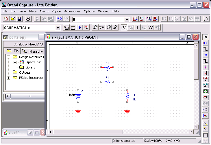
After adding the ANALOG and SOURCE libraries, resistors, capacitors, inductors and voltage and current sources become available.

To place a resistor on the schematic, first select it from the ANALOG library as shown next.
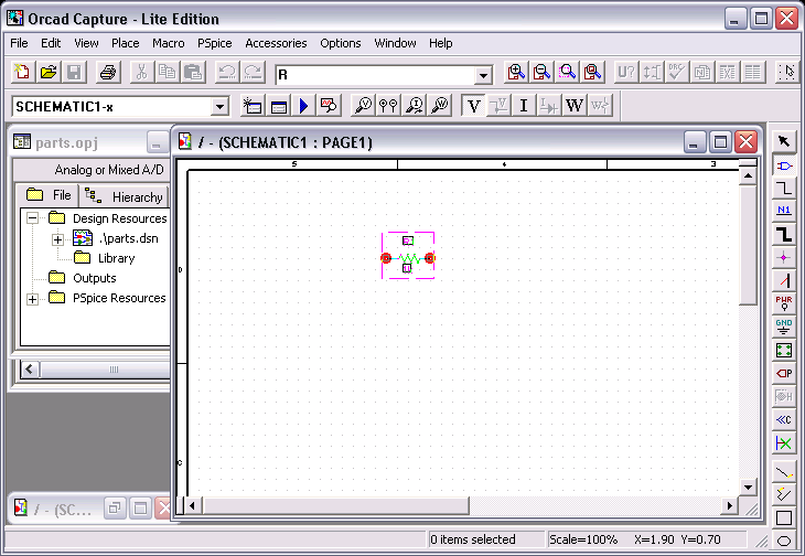
Then click on "OK". Now move the resistor to the desired location on the schematic and click to drop it.
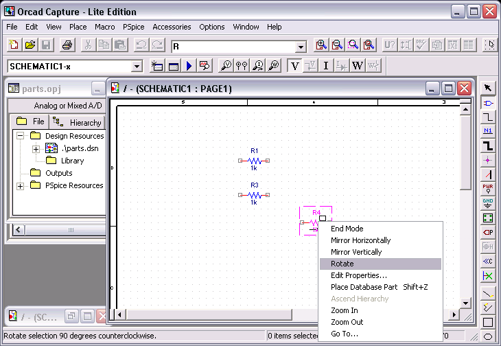
To place more parts of the same type, move to the next location and click again at the location where you want the part to go. To rotate, mirror, or flip a part, or to end placing parts of this type right-click on the schematic and select the appropriate option.
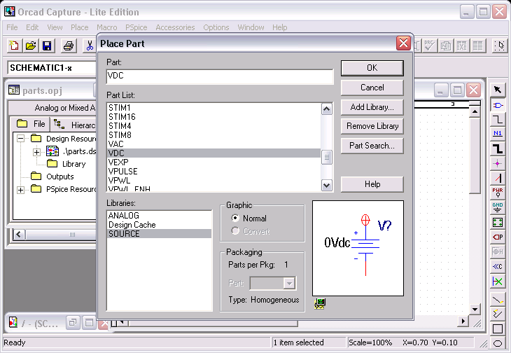
Voltage and current sources are in the SOURCES library. The following figure shows the selection of a dc voltage source (or battery).
IMPORTANT. Every PSpice project needs a PSpice Ground to
establish a reference potential. The PSpice Ground has symbol ![]() , which is different
from ordinary ground with symbol
, which is different
from ordinary ground with symbol ![]() . To get the PSpice Ground part, first click on "Place"
and then select "Ground...". You may have to add the PSpice SOURCE library
(PSpice/source.olb). Then select part "0" as shown below.
. To get the PSpice Ground part, first click on "Place"
and then select "Ground...". You may have to add the PSpice SOURCE library
(PSpice/source.olb). Then select part "0" as shown below.

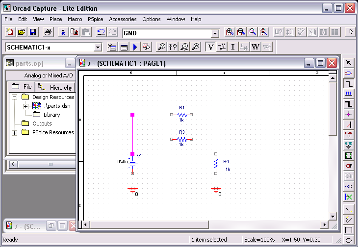
Place as many PSpice Grounds as needed. Now your schematic is ready for wiring.
To enable wiring mode, click on "Place" and then select "Wire", or click on the third vertical toolbar button. Wires ar placed by clicking at the starting node, if necessary at corners along the way, and then again at the end node.
To remove a wire or a part, select it and press the delete (Del) key. The next figure shows the circuit diagram, wired as a voltage divider. Note the Off-Page Connector (selected under "Part" and "Off-Page Connector...") which has been added to show the output of the circuit explicitly.

Finally, a title is added to the circuit (click on "Place" and select "Text..."), the output connector is relabeled, and the desired element values are entered. To change the value of an element, double-click on the current value and enter the new value. The completed circuit, which is ready for analysis in PSpice, is shown in the following figure.

The following figure shows the PSpice libraries that are available on Orcad 9.2 Lite Edition.
The most important libraries for Cicuits 1 and 2 are analog.olb, breakout.olb, eval.olb, source.olb, and special.olb. The next figure shows the most commonly used parts and the libraries from which they are available.

Numerical values for parts can be integers (5, -12, 15) or real numbers (-1.75, 3.1415, 0.7071). In either case the numbers can be followed by an integer exponent (1E6, 2.2e-9) or by a symbolic scale factor (530u, 1.2meg). These scale dactors are summarized in the following table.
| Letter Suffix | Multiplying Factor | Name of Suffix |
|---|---|---|
| T or t | 1e12 | tera |
| G or g | 1e9 | giga |
| MEG or meg | 1e6 | mega |
| K or k | 1e3 | kilo |
| M or m | 1e-3 | milli |
| U or u | 1e-6 | micro |
| N or n | 1e-9 | nano |
| P or p | 1e-12 | pico |
| F or f | 1e-15 | femto |
Letters which are not sclae factors and which immediately follow either a number or a scale factor are ignored. Thus, 12, 12V, 12A, 12Hz, 12H all represent the same number. Similarly 3.3m, 3.3mOhm, 3.3mV, 3.3MOhm all represent the number 3.3e-3 or 0.0033. Note: A resistor value of 3.3 megaohm is entered in PSpice as 3.3meg or 3.3megohm or 3.3MEGohm, but not as 3.3MOhm.
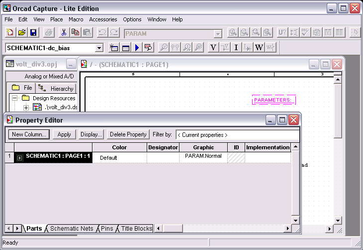
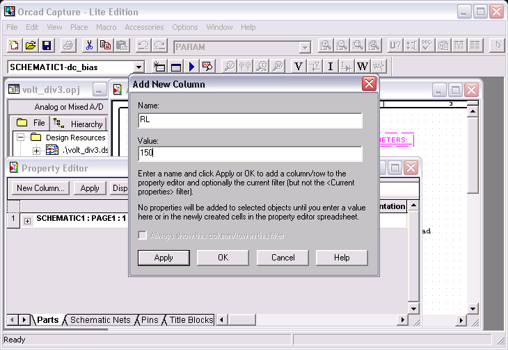
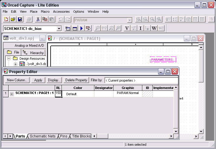
Select any element and right-click on it. In the window that pops up choose "Edit Properties..." to launch the property editor. This is shown for a resistor in the following figure.

Resistors are usually assumed to be perfect in PSpice. But the resistor model can be altered to specify a resistor tolerance, e.g., 10% as shown below.

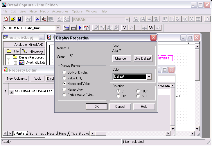
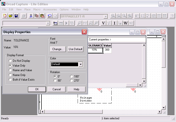
To show the tolerance explicitly in the schematic, select the "Tolerance" field in the Property Editor and then click on "Display..." to bring up a Display Properties window as shown below.

Select the desired Display Format and then click "OK"
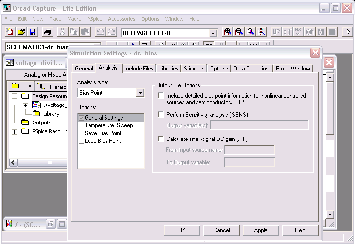
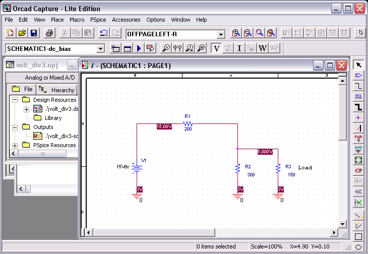
The simplest type of circuit analysis with PSpice is a dc bias point analysis. For this analysis only the parts of the circuit that are affected by dc voltages and currents are simulated in PSpice. The results that are obtained from a dc bias point analysis are the dc voltages across all elements, the dc currents through all elements, and the power absored or delivered by each element. As an example, start from the voltage divider circuit shown below.
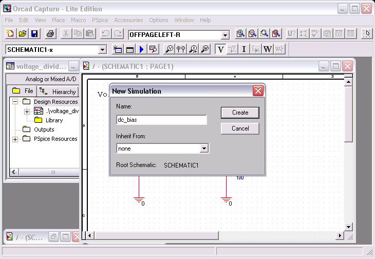
To set up a PSpice simulation, click on "PSpice" and then select "New Simulation Profile". Enter a filename for the simulation, e.g., dc_bias as shown below.
Click on "Create" and then choose the "Bias Point" option in the window that pops up. Leave the checkmark options blank as shown in the next figure and then click "OK".
Now you're ready to run PSpice by selecting the menu option "PSpice" and then "Run". The output from the simulation can be a text file, a plot, or both. For the simple example used here no parameters vary and thus no plot is generated. To see the text file, select "View" and then "Output File". A portion of this is shown in the next figure.
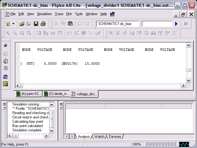
As expected, the voltage at the output connector (OUT) is 5V. A handy feature of the Orcad Capture application is that the voltages, currents, and powers computed during the Bias Point simulation can be viewed directly in the schematic as shown below.
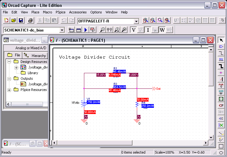
Use the "V", "I" and "W" buttons on the horizontal menu bar to turn the voltage, current, and power results on or off.
Here is the schematic of a voltage divider with IPFRINT and VPRINT1 devices to record the current into the voltage divider and the voltage at the output of the voltage divider. IPRINT and VPRINT1 are both from the SPECIAL PSpice library. Note: VPRINT1 always measures voltage with respect to (PSpice) ground. Use VPRINT2 to measure voltage between two arbitrary nodes in the circuit.
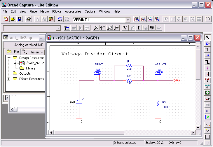
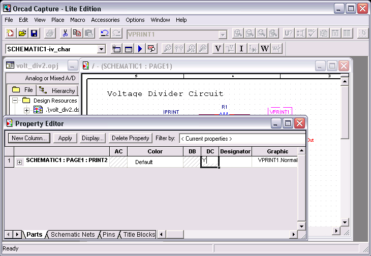
To obtain an output from IPRINT and VPRINT you need to specify what they should record. Click on the print device to select it and then right-click and select "Edit Properties...". In the Property Editor enter "Y" in the "DC" column as shown below for the VPRINT device. This tells the VPRINT device to print dc voltages. Repeat for IPRINT to print dc current.
Next, click on "PSpice" and select "New Simulation Profile". Enter a name for the simulation profile in the window that pops up.
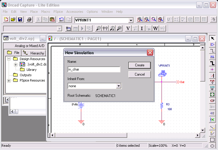
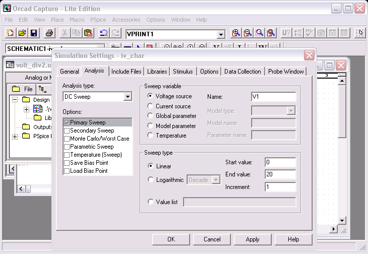
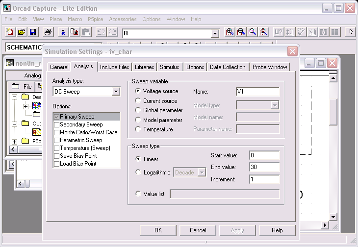
The sweep variable in this example the voltage source V1. For this example V1 is swept linearly from 0V to 20V in 1V increments.
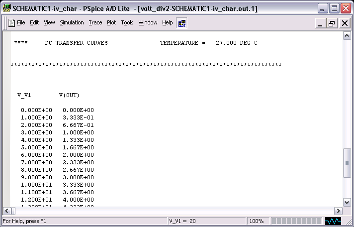
Click on "PSpice" and select "Run" to run the DC Sweep analysis. To see the results from the PRINT devices click on "View" and then select "Output File" in the PSpice result window. Scroll down to the columns headed V_V1 (the voltage of the source V1) and I(V_PRINT) (the current recorded by IPRINT).

Similarly, scroll down to the columns headed V_V1 (the voltage of the source V1) and V(OUT) (the voltage recorded by VPRINT1 at the off-page connector labeled Out).


Real resistors have tolerances, e.g. plus/minus 5% and this affects the behavior of circuits. By default the PSpice model assumes perfect resistors with resistance values exactly as specified. The voltage divider circuit below is used to show how resistor tolerances can be simulated and how a worst case analysis can be used to see to which extent these tolerances can affect the output from the circuit.

To specifiy a tolerance for a resistor, first select the resistor, then right-click on it and select "Edit Properties...". Scroll to the column labeled Tolerance and enter 10% as shown below.

To make the tolerance setting visible in the schematic, select the Tolerance field and then click on "Display...". Check the "Value Only" button as shown next.
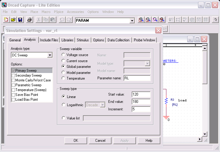
Repeat this for all resistors whose tolerances you want to take into account. Then generate a new PSpice simulation profile.
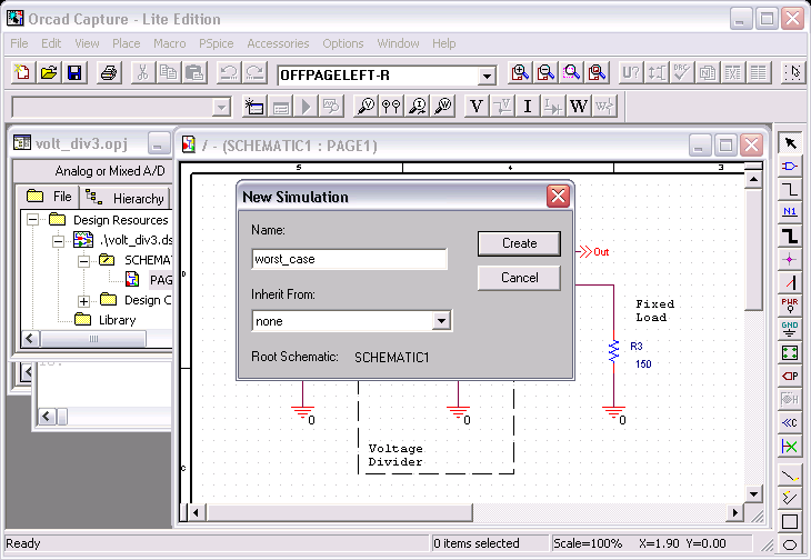
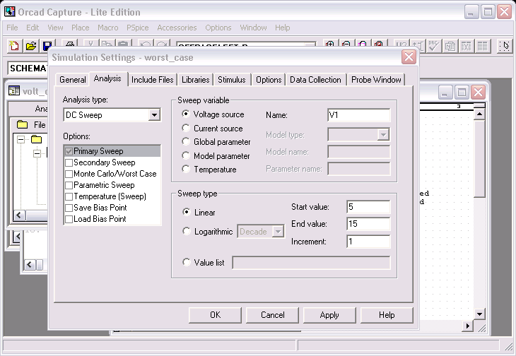
Select "DC Sweep" for the Analysis type and fill in values for the desired range of input voltages (or currents).
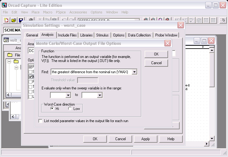
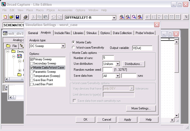
Next choose the Monte Carlo/Worst Case Option and select the "Worst-case/Sensitivity" button. Specify the output variable and choose to vary devices that have device tolerances only (no LOT tolerances).
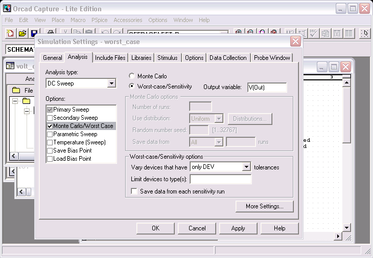
Click on the "More Settings..." button and specify the function to be performed (YMAX, MAX, MIN) by the simulation and the Worst-Case direction (Hi or Low).
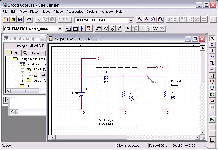
Here is the schematic of the voltage divider, ready for worst-case simulation. The goal is to find out what the output voltage will be for the worst combination of resistance values for R1 and R2 within the specified 10% tolerance.
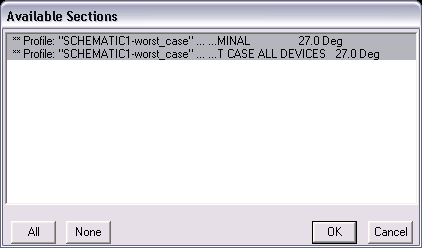
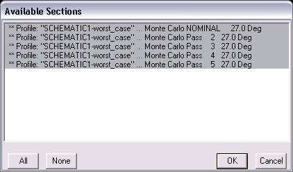
After the simulation you have to choose which results should be displayed in the plot window. The Available Sections shown below are NOMINAL and WORST CASE ALL DEVICES. Select both so that you can see the difference between the output of the ideal and the real (with tolerances) circuit.
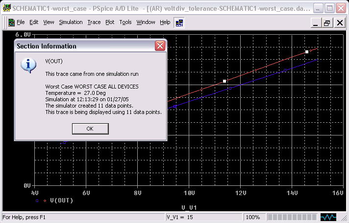
To see where a particular trace came from, right-click on it and select "Information".
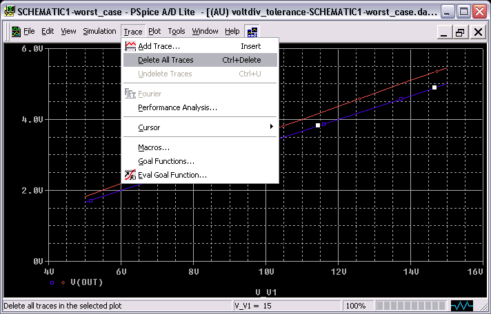
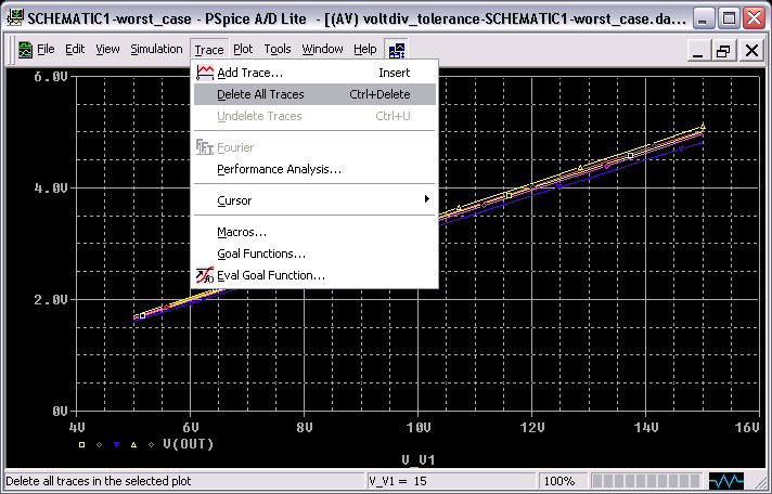
Now suppose that rather than displaying V(OUT) versus V_V1, you'd be interested in plotting the ratio V(OUT)/V(IN). To do this, first select "Trace" and then "Delete All Traces" as shown below.
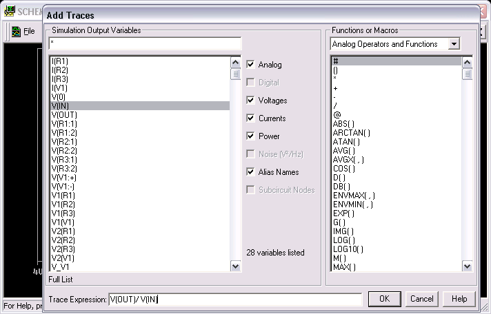
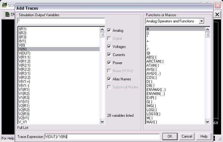
Then, again under "Trace", select "Add Trace...". Select the V(OUT) Simulation Output Variable first, then type a "/" in the Trace Expression box, followed by selecting the V(IN) Simulation Output Variable.
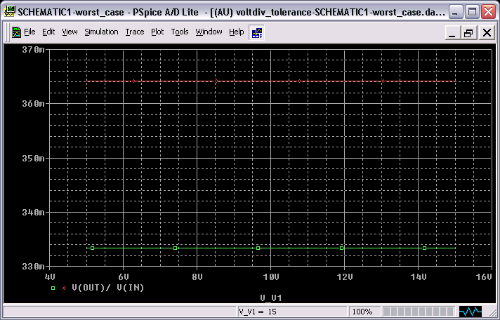
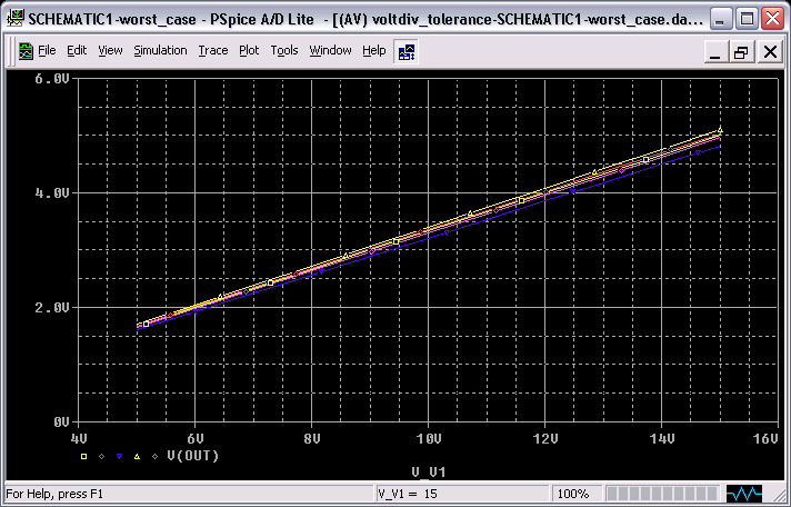
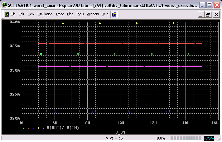
Click "OK" to obtain the following graph that shows the nominal V(OUT)/V(IN) ratio at 0.333 and the worst-case (in Hi direction) V(OUT)/V(IN) ratio at 0.364.
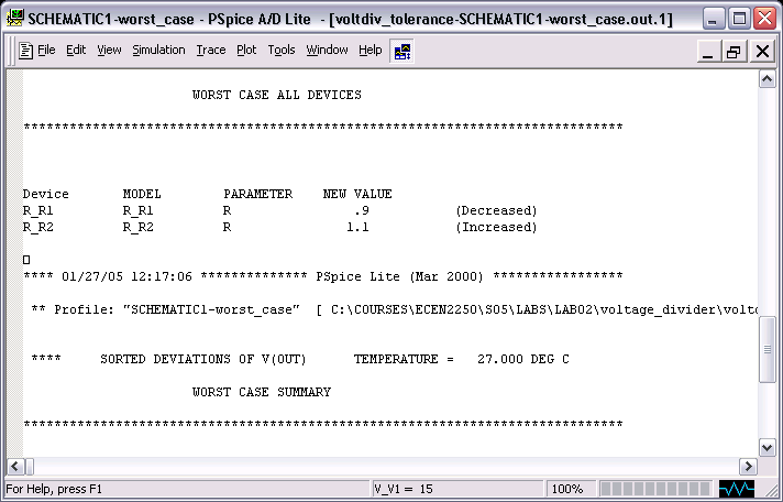
Next click on "View" and select "Output File" in the PSpice probe window to see the parameters of the worst-case analysis. The screen snapshot below shows the worst-case device values (in Hi direction). Not too surprisingly, the value of resistor R1 is reduced by 10% whereas the value of resistor R2 is increased by 10%.
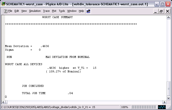
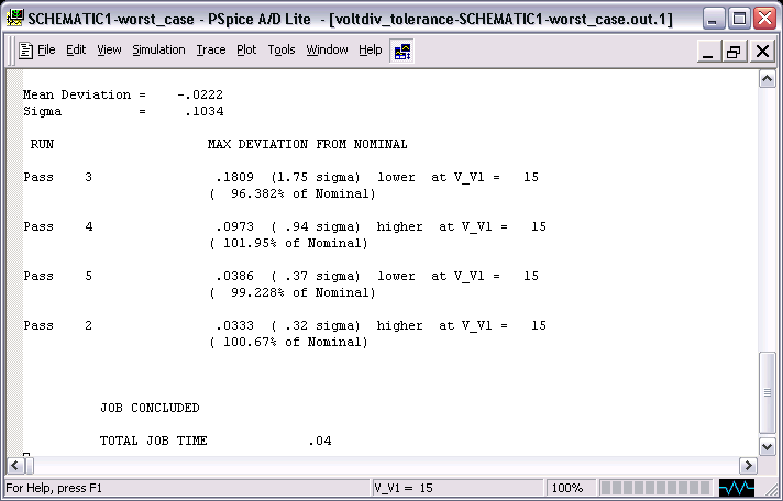
Finally, the next figure shows the summary of the worst-case analysis. It shows that the output voltage is 0.4636 V higher (than the nominal value of 5 V) for the worst combination of resistance deviations due to resistor tolerances.
-- To be completed --
-- To be completed --